.jpg)
.jpg) |
.jpg) |
.jpg) |


|
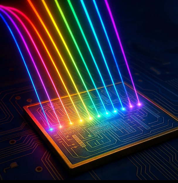
광으로 계산하는 시대가 온다: 100개 파장으로 동시에 연산하는 차세대 광 컴퓨팅 칩 | |||
| 2025년, 중국의 한 연구팀이 세계적인 과학 저널 《Nature Pho... |
 |  |
 |
광으로 계산하는 시대가 온다: 100개 파장으로 동시에 연산하는 차세대 광 컴퓨팅 칩
디지털의 한계에 도전하는 ‘빛의 계산’
인공지능의 연산 능력은 놀라운 속도로 발전하고 있지만, 그만큼 계산에 소모되는 전력과 발열도 함께 증가하고 있다. 채팅봇 하나를 작동시키기 위해 수천 개의 GPU가 가동되고, 대형 데이터센터는 마치 발전소처럼 전력을 소비한다. 전자 기반 컴퓨터는 분명한 한계를 향해 달려가고 있는 셈이다. 이 문제를 근본적으로 해결할 수 있는 새로운 방식으로 떠오른 것이 바로 '광 컴퓨팅(photonic computing)', 즉 '빛으로 계산하는 기술'이다.
2025년, 중국의 한 연구팀이 세계적인 과학 저널 《Nature Photonics》에 획기적인 연구를 발표했다. '100개의 서로 다른 빛의 파장(색깔)을 이용해 동시에 계산할 수 있는 광컴퓨팅 칩'을 개발한 것이다. 단일 칩에서 이처럼 많은 채널을 동시에 작동시키는 것은 최초의 사례이며, 이는 전자 대신 빛으로 연산을 처리하는 시대가 멀지 않았음을 시사한다.
왜 '빛'이 전자보다 빠른가?
빛은 전자보다 훨씬 빠르게 이동하며, 마찰이나 저항 없이 매질을 통과한다. 이는 열을 발생시키지 않으며, 에너지 손실이 극히 적다는 뜻이다. 또한 서로 다른 파장의 빛(예: 빨간색, 초록색, 파란색)은 '서로 간섭하지 않고 동시에 처리'될 수 있다. 이러한 특성 덕분에, 빛은 이론적으로 무수히 많은 계산을 동시에 처리할 수 있는 '병렬성'을 갖춘 매체로 주목받고 있다.
이러한 개념은 이제 실험실을 넘어 '하드웨어 수준에서 실현 가능한 기술'로 구체화되고 있다. 이번에 개발된 광컴퓨팅 칩은 전통적인 컴퓨터 칩과는 완전히 다른 구조를 갖고 있으며, 두 가지 핵심 기술이 결합되어 있다: '솔리톤 마이크로콤'과 '마하-젠더 간섭기 메쉬'.
#솔리톤 마이크로콤 (Soliton Microcomb)
이것은 하나의 빛줄기(레이저)를 수십 개의 다른 파장으로 나누어주는 ‘빛의 분배기’다. 마치 하나의 광원이 여러 색깔의 빛을 동시에 만들어내는 것처럼, '각기 다른 파장을 가진 수십 개의 계산 경로'를 생성해준다. 이 파장들은 각기 독립적으로 움직이며, 각각 하나의 계산 회로처럼 작동한다.
쉽게 말해, 일반 컴퓨터는 1차선 도로에서 차량 한 대가 순서대로 지나가는 방식이라면, 이 기술은 '100차선 고속도로를 만들어 동시에 100대의 차량을 통과시키는 것'에 비유할 수 있다.
#마하-젠더 간섭기 (Mach–Zehnder Interferometer)
이 장치는 '빛을 나눠서 서로 다른 경로로 이동시킨 후 다시 합쳐서, 그 차이를 이용해 계산하는 구조'다. 물리학에서는 ‘간섭’을 통해 파동의 위상 차이를 계산하는 데 자주 사용된다. 이번 연구에서는 이 구조를 수십 개 이상 격자처럼 배열해, 각 파장이 마치 뉴런처럼 계산을 수행하도록 설계했다.
쉽게 말하자면, 마하-젠더 간섭기는 '빛의 경로를 바꾸고, 더하고, 비교하는 '스위치+계산기' 역할'을 한다고 보면 된다.
성능의 전환점: GPU보다 30,000배 효율적?
이번 광컴퓨팅 칩은 'GPU보다 전력 효율이 최대 30,000배 이상 높다'는 가능성을 보여주었다. 실제로, 기존의 전자기 기반 딥러닝 연산에서는 연산에 사용되는 에너지의 대부분이 ‘열’로 소모된다. 반면 광 기반 연산은 에너지 손실이 거의 없으며, 냉각 장치 없이도 안정적으로 작동할 수 있다.
뿐만 아니라, 빛은 전자보다 훨씬 빠른 속도로 움직이기 때문에 '딥러닝의 핵심인 대용량 행렬 곱셈을 실시간에 가깝게 수행할 수 있다.' 특히 이미지 인식, 실시간 번역, 자율주행차의 센서 신호 해석 등에서 '즉각적인 반응 속도가 요구되는 분야'에서 탁월한 성능을 기대할 수 있다.
한국이 왜 이 기술에 주목해야 하는가?
1. 시스템 반도체의 기회
한국은 메모리 반도체에서는 세계적인 강국이지만, 'GPU나 AI 칩 같은 시스템 반도체 분야는 상대적으로 약하다.' 그러나 광컴퓨팅처럼 패러다임이 바뀌는 순간에는, 후발주자에게도 기회가 열린다. 이는 과거 스마트폰 초기에 한국이 삼성·LG를 통해 글로벌 플레이어로 부상한 것과 비슷한 전환의 시점이다.
2. 통신과 센서 산업의 연계 가능성
한국은 이미 '광통신, 센서, 정밀 광학 기기 분야에서 세계적 인프라와 인재를 확보'하고 있다. 이번 광칩 기술은 이런 기존 산업과의 연계성이 높으며, 'AI 연산, 통신, 센싱 기술을 동시에 발전'시킬 수 있는 교차점에 위치한다.
3. 국가 차원의 저전력 전략과도 부합
정부는 탄소중립과 디지털 전환을 동시에 추진하고 있다. 그러나 AI와 디지털 기술은 기본적으로 에너지를 많이 쓰는 구조다. 이 딜레마 속에서 광컴퓨팅은 '디지털 혁신과 에너지 절감이라는 두 마리 토끼를 동시에 잡을 수 있는 기술'이다.
전망: 실용화까지 얼마나 남았나?
현재의 기술은 프로토타입 수준이다. 칩 하나에 100개 파장을 얹었지만, 이를 수천 개로 늘리는 작업, 대규모 연산에 맞는 인터페이스 설계, 기존 소프트웨어와의 호환 등 여러 과제가 남아 있다. 그러나 기술의 방향성은 분명하다. 불과 몇 년 전만 해도 실험실에서 간신히 빛을 나누던 수준이었지만, 이제는 '칩 하나에 정밀 제어가 가능한 연산 광학 구조'를 집적할 수 있는 시대가 왔다.
이 기술이 양산화된다면, 우리는 '전력 소모가 거의 없는 AI 칩', '빛으로 동작하는 모바일 디바이스', 심지어 '인체 삽입형 광 기반 뉴럴 컴퓨터'까지도 상상할 수 있다. 현실이 되는 것은 시간의 문제다.
광컴퓨팅은 선택이 아닌 전략이다
이번 연구는 한 국가의 과학 성과에 그치지 않는다. 이는 전 세계가 직면한 '계산 효율성의 위기', 'AI 에너지 소비 증가', '반도체 산업의 구조적 포화'라는 문제에 대한 하나의 전략적 해법이다. 그리고 이 해법은, 우연히도 한국이 강점을 가진 산업들과 긴밀히 연결되어 있다.
지금이야말로 한국이 이 기술의 ‘사용자’가 아닌 '선도자'로 전환할 수 있는 기회'다. 정부, 대학, 민간기업이 이 기술에 대한 장기적 로드맵을 갖고 협업을 시작한다면, '광으로 생각하는 컴퓨터'는 상상이 아니라 현실이 될 것이다.
* Reference
Nature Photonics, June 2025, “Massively parallel photonic computing with 100 wavelength channels using a soliton microcomb and Mach–Zehnder mesh,” Zhang et al.